- 您现在的位置:买卖IC网 > Sheet目录341 > MAX8811EEE+ (Maxim Integrated)IC DRVR DL PHASE HS 16-QSOP
�� �
�
�High-Speed,� Dual-Phase� Driver� with�
�Integrated� Boost� Diodes�
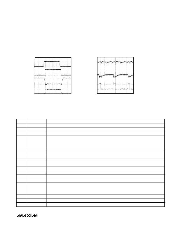
�Typical� Operating� Characteristics� (continued)�
�(V� VL1� =� V� VL2� =� V� EN� =� V� DLY� =� 6.5V,� 3000pF� capacitive� load,� T� A� =� +25°C,� unless� otherwise� noted.)�
�SWITCHING� WAVEFORMS�
�MAX8811toc09�
�VPWM�
�5V/div�
�VLX�
�10V/div�
�VDL�
�5V/div�
�VBST_� AND� VL_� WAVEFORMS�
�MAX8811toc10�
�VL� (AC-COUPLED)�
�500mV/div�
�VBST� (AC-COUPLED)�
�200mV/div�
�100ns/div�
�VDH�
�5V/div�
�f� SW� = 250kHz�
�1� μ� s/div�
�VLX�
�10div�
�Pin� Description�
�PIN�
�1�
�2�
�3�
�4�
�5�
�6�
�7�
�8�
�9�
�10�
�11�
�12�
�13�
�14�
�15�
�16�
�NAME�
�BST1�
�DH1�
�LX1�
�VL1�
�DL1�
�PGND1�
�EN�
�DLY�
�PWM1�
�PWM2�
�PGND2�
�DL2�
�VL2�
�LX2�
�DH2�
�BST2�
�FUNCTION�
�Boost Capacitor Connection for Phase 1. Connect a 0.22μF ceramic capacitor between BST1 and LX1.�
�High-Side� Gate-Driver� Output� for� Phase� 1.� DH1� is� pulled� low� during� shutdown� and� UVLO.�
�Inductor� Connection� for� Phase� 1�
�Gate-Drive� Supply� for� DL1.� Connect� VL1� to� a� 4.5V� to� 7V� supply.� VL1� must� be� connected� to� VL2�
�externally.� Bypass� the� VL1/VL2� connection� with� a� 2.2μF� or� larger� ceramic� capacitor� to� the� power� ground�
�plane.�
�Low-Side� Gate-Driver� Output� for� Phase� 1.� DL1� is� pulled� low� during� shutdown� and� UVLO.�
�Power� Ground� for� DL1.� Connect� PGND1� and� PGND2� to� the� power� ground� plane� at� the� IC.�
�Enable� Input.� Drive� EN� high� for� normal� operation,� or� low� for� shutdown.�
�Delay� Time� Setting� Input.� Connect� a� resistor� from� DLY� to� PGND1� to� set� the� dead� time� between� DL� falling�
�and� DH� rising,� or� connect� DLY� to� VL1� to� use� the� default� delay.�
�PWM� Logic� Input� for� Phase� 1.� DH1� is� high� when� PWM1� is� high;� DL1� is� high� when� PWM1� is� low.�
�PWM� Logic� Input� for� Phase� 2.� DH2� is� high� when� PWM2� is� high;� DL2� is� high� when� PWM2� is� low.�
�Power� Ground� for� DL2.� Connect� PGND1� and� PGND2� to� the� power� ground� plane� at� the� IC.�
�Low-Side� Gate-Driver� Output� for� Phase� 2.� DL2� is� pulled� low� during� shutdown� and� UVLO.�
�Gate-Drive� Supply� for� DL2.� Connect� VL2� to� a� 4.5V� to� 7V� supply.� VL1� must� be� connected� to� VL2�
�externally.� Bypass� the� VL1/VL2� connection� with� a� 2.2μF� or� larger� ceramic� capacitor� to� the� power� ground�
�plane.�
�Inductor� Connection� for� Phase� 2�
�High-Side� Gate-Driver� Output� for� Phase� 2.� DH2� is� pulled� low� during� shutdown� and� UVLO.�
�Boost� Capacitor� Connection� for� Phase� 2.� Connect� a� 0.22μF� ceramic� capacitor� between� BST2� and� LX2.�
�_______________________________________________________________________________________�
�5�
�发布紧急采购,3分钟左右您将得到回复。
相关PDF资料
MAX8821ETI+
IC LED DRVR WHITE BCKLGT 28-TQFN
MAX8822ETE+T
IC LED DRVR WHITE BCKLGT 16-TQFN
MAX8830EWE+T
IC LED DRVR WHITE BCKLGT 16-UCSP
MAX8831EWE+T
IC LED DRIVR WHITE BCKLGT 16-WLP
MAX8834ZEWP+T
IC LED DRIVR BCKLGT FLASH 20-WLP
MAX8855EVKIT+
KIT EVAL FOR MAX8855
MAX8879ETG+T
IC LED DRVR WT/RGB BCKLGT 24TQFN
MAX8901BETA+TCH8
IC LED DRIVER WHITE BCKLGT 8TDFN
相关代理商/技术参数
MAX8811EEE+T
功能描述:功率驱动器IC High-Speed Dual Phase Driver RoHS:否 制造商:Micrel 产品:MOSFET Gate Drivers 类型:Low Cost High or Low Side MOSFET Driver 上升时间: 下降时间: 电源电压-最大:30 V 电源电压-最小:2.75 V 电源电流: 最大功率耗散: 最大工作温度:+ 85 C 安装风格:SMD/SMT 封装 / 箱体:SOIC-8 封装:Tube
MAX8814ETA+
制造商:Maxim Integrated Products 功能描述:CHGR LI-ION/LI-POL 570MA 4.2V 8TDFN EP - Rail/Tube 制造商:Rochester Electronics LLC 功能描述:
MAX8814ETA+T
功能描述:电池管理 28V Linear Li+ Battery Charger RoHS:否 制造商:Texas Instruments 电池类型:Li-Ion 输出电压:5 V 输出电流:4.5 A 工作电源电压:3.9 V to 17 V 最大工作温度:+ 85 C 最小工作温度:- 40 C 封装 / 箱体:VQFN-24 封装:Reel
MAX8814EVKIT+
功能描述:电源管理IC开发工具 MAX8814 Eval Kit
RoHS:否 制造商:Maxim Integrated 产品:Evaluation Kits 类型:Battery Management 工具用于评估:MAX17710GB 输入电压: 输出电压:1.8 V
MAX8815AETB+
制造商:Maxim Integrated Products 功能描述:1A 97% EFFICIENCY 30UA QUIESCENT 制造商:Maxim Integrated Products 功能描述:1A, 97% EFFICIENCY, 30?A QUIESCENT CURRENT, STEP-UP CONVERTE - Bulk
MAX8815AETB+T
功能描述:直流/直流开关转换器 Step-Up DC/DC Converter
RoHS:否 制造商:STMicroelectronics 最大输入电压:4.5 V 开关频率:1.5 MHz 输出电压:4.6 V 输出电流:250 mA 输出端数量:2 最大工作温度:+ 85 C 安装风格:SMD/SMT
MAX8815AEVKIT+
功能描述:DC/DC 开关控制器 Evaluation Kit for the MAX8815A RoHS:否 制造商:Texas Instruments 输入电压:6 V to 100 V 开关频率: 输出电压:1.215 V to 80 V 输出电流:3.5 A 输出端数量:1 最大工作温度:+ 125 C 安装风格: 封装 / 箱体:CPAK
MAX8818AETM+
功能描述:PMIC 解决方案 10Ch PMIC for 2-Cell Li+ DVC System RoHS:否 制造商:Texas Instruments 安装风格:SMD/SMT 封装 / 箱体:QFN-24 封装:Reel